|
Title: Is an 80% decrease in power consumption possibe when going from 110nm to 65nm? Post by: Fuzzy on January 31, 2013, 04:55:09 AM Crunching some power consumption numbers here and a little skeptical at BFL's specs showing 1W/Gh, considering Avalon gets about
Anyone here familiar enough with chip design to weight in on this? EDIT: Looks like Avalon falsified their real world numbers on their site, even after the fist machine was already in customers' hands. They updated them to "reflect customers' experience" to 620w for a 66Gh/s rig. Title: Re: Is an 80% decrease in power consumption possibe when going from 110nm to 65nm? Post by: mb300sd on January 31, 2013, 05:00:46 AM 130nm = pentium 3
65nm = core 2 duo sounds possible Title: Re: Is an 80% decrease in power consumption possibe when going from 110nm to 65nm? Post by: dust on January 31, 2013, 05:01:20 AM Comparing the squares of the process size should be a decent measure of efficiency, if everything else is similar. (110/65)^2 = 2.86x more efficient. The rest of the advantage would come from a more efficient design. If BFL's chips are "full custom" as they say, this could lead to additional gains over Avalon.
Title: Re: Is an 80% decrease in power consumption possibe when going from 110nm to 65nm? Post by: DeathAndTaxes on January 31, 2013, 05:11:50 AM dust got it right. If it was exactly the same chip one would expect closer to 2x to 3x better efficiency. A lot will depends on the exact design. Personally I think Avalon went the right route. Any ASIC is far superior to GPU so use 110nm, get a simple working design out the door. A couple million in sales later you got plenty of money to do an improved design maybe tweak out 50% to 100% improvement in efficiency at the same 110nm, and THEN make a move to smaller process. If your competitors are crushing you then you can either jump to 65nm or take a gamble on more efficient design AND a jump to 65nm on the same chip. Get the most out of your resources and leave yourself options to improve. Note this strategy is called tick-tock and is used by Intel. Intel used it to good effect to utterly destroy AMD.
Tick - do a die shrink Tock - improve the efficiency (2nd gen design on same die size). For the record I don't think BFL is a "scam" but my guess is 1000 MH/J is the high end of their range. With real world inefficiencies, power consumption rising due to ambient temps, power supply inefficiency, and simple variance in chip yields I think they will underperform that number. Note probably not 500MH/J vs 1000 MH/J but maybe 10% to 20% below. Note the following is a totally hypothetical example made up completely for my amusement. Tick - 110nm Avalon (160 MH/J) Tock - 110nm Improved Avalon (280 MH/J) Tick - 65nm XXXX (560 MH/J) <- improved avalon design die shrinked to 65nm Tock - 65nm XXX (800 MH/J) Title: Re: Is an 80% decrease in power consumption possibe when going from 110nm to 65nm? Post by: Bogart on January 31, 2013, 05:26:04 AM dust got it right. If it was exactly the same chip one would expect closer to 2x to 3x better efficiency. A lot will depends on the exact design. Personally I think Avalon went the right route. Any ASIC is far superior to GPU so use 110nm, get a simple working design out the door. A couple million in sales later you got plenty of money to do an improved design maybe tweak out 50% to 100% improvement in efficiency, and THEN make a move to smaller process. Get the most out of your resources. Note this strategy is called tick-tock and is used by Intel. Mm hmm. I used to work at a tech company for a boss who was famous within the company for his slogan "Ship it!". He'd say it, and we'd do it. We shipped some hacked-together shit, and boy it's a good thing we did. In retrospect, "ship it" was absolutely the right decision to have made every time. It was far better to get something out the door that halfway worked, and to fix it better later than to delay and have nothing out there while we tried and tried again for perfection. This went double for the confidence of our customers. They by far preferred to see us doing something and getting something into their hands, even if it was hacked. </tangent> Title: Re: Is an 80% decrease in power consumption possibe when going from 110nm to 65nm? Post by: Fuzzy on January 31, 2013, 05:32:59 AM I used to work at a tech company for a boss who was famous within the company for his slogan "Ship it!". He'd say it, and we'd do it. We shipped some hacked-together shit, and boy it's a good thing we did. In retrospect, "ship it" was absolutely the right decision to have made every time. It was far better to get something out the door that halfway worked, and to fix it better later than to delay and have nothing out there while we tried and tried again for perfection. This went double for the confidence of our customers. They by far preferred to see us doing something and getting something into their hands, even if it was hacked. </tangent> Are you saying that the Avalon ASIC is "hacked-together shit" that only "halfway work(s)" shipped out just to "getting something into [the customers'] hands" ?? That sounds about right, but it's still the best (first) ASIC "on the market". ;) Title: Re: Is an 80% decrease in power consumption possibe when going from 110nm to 65nm? Post by: Nemesis on January 31, 2013, 06:20:23 AM dust got it right. If it was exactly the same chip one would expect closer to 2x to 3x better efficiency. A lot will depends on the exact design. Personally I think Avalon went the right route. Any ASIC is far superior to GPU so use 110nm, get a simple working design out the door. A couple million in sales later you got plenty of money to do an improved design maybe tweak out 50% to 100% improvement in efficiency at the same 110nm, and THEN make a move to smaller process. If your competitors are crushing you then you can either jump to 65nm or take a gamble on more efficient design AND a jump to 65nm on the same chip. Get the most out of your resources and leave yourself options to improve. Note this strategy is called tick-tock and is used by Intel. Intel used it to good effect to utterly destroy AMD. Tick - do a die shrink Tock - improve the efficiency (2nd gen design on same die size). For the record I don't think BFL is a "scam" but my guess is 1000 MH/J is the high end of their range. With real world inefficiencies, power consumption rising due to ambient temps, power supply inefficiency, and simple variance in chip yields I think they will underperform that number. Note probably not 500MH/J vs 1000 MH/J but maybe 10% to 20% below. Note the following is a totally hypothetical example made up completely for my amusement. Tick - 110nm Avalon (160 MH/J) Tock - 110nm Improved Avalon (280 MH/J) Tick - 65nm XXXX (560 MH/J) <- improved avalon design die shrinked to 65nm Tock - 65nm XXX (800 MH/J) The so-called tick-tock strategy is used by many chips manufactures as well (including AMD), you make it sound like its exclusively to Intel. No, it has nothing to do with AMD's failure. This tick-tock wont work with small batchs orders. Avalon need to have streamlines in production to capitalize enough market share while being the first one ships out ASIC. Once BFL ship their ASIC (if no more delays), Avalon is doomed. BFL took a bigger risk with larger productions, hence they will have greater return if they succeed. Title: Re: Is an 80% decrease in power consumption possibe when going from 110nm to 65nm? Post by: crazyates on January 31, 2013, 06:26:57 AM dust got it right. If it was exactly the same chip one would expect closer to 2x to 3x better efficiency. A lot will depends on the exact design. Personally I think Avalon went the right route. Any ASIC is far superior to GPU so use 110nm, get a simple working design out the door. A couple million in sales later you got plenty of money to do an improved design maybe tweak out 50% to 100% improvement in efficiency at the same 110nm, and THEN make a move to smaller process. If your competitors are crushing you then you can either jump to 65nm or take a gamble on more efficient design AND a jump to 65nm on the same chip. Get the most out of your resources and leave yourself options to improve. Note this strategy is called tick-tock and is used by Intel. Intel used it to good effect to utterly destroy AMD. Tick - do a die shrink Tock - improve the efficiency (2nd gen design on same die size). Well compared to GPUs, of course the Avalon unit looks amazing! But the size, power, and cooling requirements for 20 of these is just too much. I can plan on putting 20 SC Singles in my basement with no issues whatsoever. I couldn't imagine putting 20 Avalon's down there, as the 8000Watt draw would kill me, and the heat would roast my house in the summer. Also, Intel's tick/tock (http://en.wikipedia.org/wiki/Intel_Tick-Tock) doesn't quite work that way. Tick - Die Shrink of old Architecture - Similar performance, lower power draw Tock - New Architecture - Faster performance, similar power draw Title: Re: Is an 80% decrease in power consumption possibe when going from 110nm to 65nm? Post by: crazyates on January 31, 2013, 06:33:50 AM The so-called tick-tock strategy is used by many chips manufactures as well (including AMD), you make it sound like its exclusively to Intel. No, it has nothing to do with AMD's failure. That's only partially true. Intel's tick/tock was planned out to die shrink one year, and then release a new architecture the next. Rinse and repeat. They wanted either a tick or a tock every year, setting a very aggressive pace for themselves.AMD only sometimes separates these out. For example, the K10 family started as 65nm, but shrunk to 45nm. However, when they released the FX series, they did both - new architecture (FX), and smaller die size (32nm). Title: Re: Is an 80% decrease in power consumption possibe when going from 110nm to 65nm? Post by: hardcore-fs on January 31, 2013, 07:57:24 AM Comparing the squares of the process size should be a decent measure of efficiency, if everything else is similar. (110/65)^2 = 2.86x more efficient. The rest of the advantage would come from a more efficient design. If BFL's chips are "full custom" as they say, this could lead to additional gains over Avalon. Only if BOTH designs have been professionally implemented. Title: Re: Is an 80% decrease in power consumption possibe when going from 110nm to 65nm? Post by: Fuzzy on February 01, 2013, 04:53:57 PM With real world inefficiencies, power consumption rising due to ambient temps, power supply inefficiency, and simple variance in chip yields I think they will underperform that number. Note probably not 500MH/J vs 1000 MH/J but maybe 10% to 20% below. That'll be fine for most of their units, but the Mini-rig is already sitting at 1500w. Considering a standard wall plug is only good for 1650w, there's not much room for failure there. Title: Re: Is an 80% decrease in power consumption possibe when going from 110nm to 65nm? Post by: MrTeal on February 01, 2013, 04:59:40 PM With real world inefficiencies, power consumption rising due to ambient temps, power supply inefficiency, and simple variance in chip yields I think they will underperform that number. Note probably not 500MH/J vs 1000 MH/J but maybe 10% to 20% below. That'll be fine for most of their units, but the Mini-rig is already sitting at 1500w. Considering a standard wall plug is only good for 1650w, there's not much room for failure there. Title: Re: Is an 80% decrease in power consumption possibe when going from 110nm to 65nm? Post by: creativex on February 01, 2013, 05:36:12 PM It's laughable that now that ASICs are in the wild some are calling the only shipping product an inefficient power hog. Mostly because it's being compared to a theoretical product that hasn't left the fab yet after EIGHT MONTHS of alleged work.
Avalon did this right. Create a product that's do-able, ship it and *THEN* work on increasing performance and efficiency. Title: Re: Is an 80% decrease in power consumption possibe when going from 110nm to 65nm? Post by: Luno on February 01, 2013, 06:33:09 PM I don't think that differences in power efficiencies between the two technologies really is a strong selling point.
A difference of running costs of 2.86, as suggested, is important if you are running a farm. However if the average customer only buys a single device the pricetag is more important. Remember that a 5830 which almost used twice as much power per GPU, compared to a 5970, had the same resale value per Mhash. Title: Re: Is an 80% decrease in power consumption possibe when going from 110nm to 65nm? Post by: Fuzzy on February 01, 2013, 06:51:11 PM At $0.1/KWh, the 450w Avalon will cost $34/mo to run.
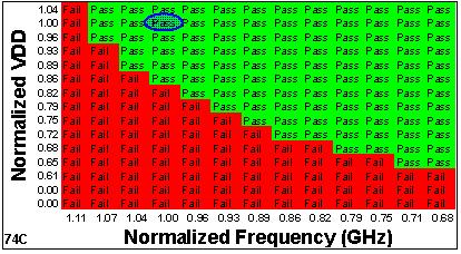
An SC Single will cost (assuming 60w) $4.50/mo. That's about a $350 difference at the end of the year. You'd make way more getting either rig a month early. Title: Re: Is an 80% decrease in power consumption possibe when going from 110nm to 65nm? Post by: DeathAndTaxes on February 01, 2013, 06:51:12 PM With real world inefficiencies, power consumption rising due to ambient temps, power supply inefficiency, and simple variance in chip yields I think they will underperform that number. Note probably not 500MH/J vs 1000 MH/J but maybe 10% to 20% below. That'll be fine for most of their units, but the Mini-rig is already sitting at 1500w. Considering a standard wall plug is only good for 1650w, there's not much room for failure there. Well technically it is a violation of US electrical code to put more than a 80% continual load on a circuit (unless the circuit is dedicated = hardwired into the device). 120V * 15A * 80% = 1440W. Peak load is 1800W but depending on wire gauge, length, etc you likely will trip the break a little below that. Honestly something pulling over a KW of juice is an industrial piece of equipment. In most homes about the only things that pull that much are electric stove or air conditioner both of which are on dedicated circuits. Still if (and I am not making a prediction here) BFL did miss there power target I think scaling back the rig 20% or so would be better than trying to find higher end PSU and redlining the house wiring. The FPGA rig ended up looking like it would pull more than 1600W so they split those orders into two "minirigs". Personally I like the idea of smaller units rackmounted anyways. With the "upgrade" Avalon would be ~88GH for ~ 530W. Standard datacenter rack could still hold 880 GH/s and use ~5.3KW or power. A locking L6-30R outlet on a 240V, 30A circuit and a PDU would allow a safe, neat, and efficient setup while still being electrical code compliant. Title: Re: Is an 80% decrease in power consumption possibe when going from 110nm to 65nm? Post by: Puppet on February 02, 2013, 08:16:33 AM Comparing the squares of the process size should be a decent measure of efficiency, if everything else is similar. (110/65)^2 = 2.86x more efficient. The rest of the advantage would come from a more efficient design. If BFL's chips are "full custom" as they say, this could lead to additional gains over Avalon. Thats about correct for dynamic power, but not for static power (leakage). Then again, for bitcoin ASICs, its probably fair to assume static power will be low enough to ignore completely. The key here is voltage. A smaller process allows lower voltages and power consumption scales with the square of voltage. But there are other ways to lower voltage significantly, not in the least lowering the clocks a little bit. A shmoo plot shows stable clocks for a given voltage. Here is an example: http://it.emcelettronica.com/files/u4/microcontrollori-frequenza-funzionamento.JPG As you can see in the above example, if you sacrifice a little top frequency, you can get away with a disproportionately lower voltage, which results in an even more significant power reduction because of the squaring. Most overclockers among us will be well aware of these effects from over/undervolting our GPUs and CPUs. BTW you cant reliably do this sort of chip qualification until you have working silicon, which makes me wonder when BFL expects to do stuff like that... Title: Re: Is an 80% decrease in power consumption possibe when going from 110nm to 65nm? Post by: lastbit on February 03, 2013, 06:50:00 PM Comparing the squares of the process size should be a decent measure of efficiency, if everything else is similar. (110/65)^2 = 2.86x more efficient. The rest of the advantage would come from a more efficient design. If BFL's chips are "full custom" as they say, this could lead to additional gains over Avalon. There's an approximation of 110/65 = 1.69x reduction in linear dimensions which translates in shorter propagation time so greater maximum frequency. I know smaller the node, smaller the gain, but I'd say between these nodes (110 and 65mn) maybe there's a 1.3x speed gain. So, maybe a 2.86 x 1.3 = 3.7x only from "shrink". Title: Re: Is an 80% decrease in power consumption possibe when going from 110nm to 65nm? Post by: MrTeal on February 03, 2013, 07:04:47 PM Comparing the squares of the process size should be a decent measure of efficiency, if everything else is similar. (110/65)^2 = 2.86x more efficient. The rest of the advantage would come from a more efficient design. If BFL's chips are "full custom" as they say, this could lead to additional gains over Avalon. There's an approximation of 110/65 = 1.69x reduction in linear dimensions which translates in shorter propagation time so greater maximum frequency. I know smaller the node, smaller the gain, but I'd say between these nodes (110 and 65mn) maybe there's a 1.3x speed gain. So, maybe a 2.86 x 1.3 = 3.7x only from "shrink". A smaller process might allow a higher frequency, but that won't increase efficiency. Title: Re: Is an 80% decrease in power consumption possibe when going from 110nm to 65nm? Post by: lastbit on February 03, 2013, 11:57:06 PM Comparing the squares of the process size should be a decent measure of efficiency, if everything else is similar. (110/65)^2 = 2.86x more efficient. The rest of the advantage would come from a more efficient design. If BFL's chips are "full custom" as they say, this could lead to additional gains over Avalon. There's an approximation of 110/65 = 1.69x reduction in linear dimensions which translates in shorter propagation time so greater maximum frequency. I know smaller the node, smaller the gain, but I'd say between these nodes (110 and 65mn) maybe there's a 1.3x speed gain. So, maybe a 2.86 x 1.3 = 3.7x only from "shrink". A smaller process might allow a higher frequency, but that won't increase efficiency. You might be right. If power required for the greater frequency is the same, which I believe it's true at least for the dynamic power (1/2C*V^2*f + Qtransition*f), there is an efficiency increase. But you might be wright because at 65nm leakage power becomes comparable with dynamic power (unless you use LP process, which I doubt). Title: Re: Is an 80% decrease in power consumption possibe when going from 110nm to 65nm? Post by: Fuzzy on February 04, 2013, 12:16:13 AM EDIT: Looks like avalon falsified their real world numbers on their site, even after the fist machine was already in customers' hands. They updated them to "reflect customers' experience" to 620w for a 66Gh/s rig. Given avalon's actual 9.4 W/Gh power consumption, I really doubt BFL can even accomplish 3 W/Gh, let alone 1. Title: Re: Is an 80% decrease in power consumption possibe when going from 110nm to 65nm? Post by: Puppet on February 04, 2013, 10:52:30 AM You might be right. If power required for the greater frequency is the same, which I believe it's true at least for the dynamic power (1/2C*V^2*f + Qtransition*f), there is an efficiency increase. But you might be wright because at 65nm leakage power becomes comparable with dynamic power (unless you use LP process, which I doubt). Static power/leakage is almost certainly a non issue with bitcoin asics. Simply put, static power is the power consumed (leaked) by inactive circuits. On something as complex as a cpu, most circuits are inactive most of the time, even if the cpu is working under full load, and maybe 90% of the dynamic power is consumed in like 5% of the CPU's transistors (numbers pulled out my behind). So leakage becomes a real issue, particularly when "idle". But a bitcoin ASIC is not supposed to be idle and is incomparably simpler and all circuits are there specifically to be used while mining; so Im pretty sure 90+% of the circuits will be used pretty much all the time while mining. It really doesnt matter what the rest consumes when idle. Title: Re: Is an 80% decrease in power consumption possibe when going from 110nm to 65nm? Post by: Bicknellski on June 11, 2013, 05:03:52 AM Numbers... who needs numbers.
Title: Re: Is an 80% decrease in power consumption possibe when going from 110nm to 65nm? Post by: wrenchmonkey on June 11, 2013, 05:48:43 AM They see me trollin', they hatin'...
Title: Re: Is an 80% decrease in power consumption possibe when going from 110nm to 65nm? Post by: Bicknellski on June 11, 2013, 06:18:16 AM EDIT: Looks like avalon falsified their real world numbers on their site, even after the fist machine was already in customers' hands. They updated them to "reflect customers' experience" to 620w for a 66Gh/s rig. Given avalon's actual 9.4 W/Gh power consumption, I really doubt BFL can even accomplish 3 W/Gh, let alone 1. What were the power numbers? |