

Ⅰ. Требования к подготовке ремонтной платформы/инструментов/оборудования
1. Требования к платформе:Антистатическое рабочее место для обслуживания (рабочее место необходимо заземлить), антистатический браслет и заземление.
2. Требования к оборудованию:
(1) Паяльник с постоянной температурой (350°C-380°C), заостренный наконечник паяльника используется для пайки небольших участков, таких как чип-резисторы и конденсаторы;
(2) Термофен и ремонтная станция BGA используются для разборки и сварки чипов/BGA;
(3) Мультиметр с приваренными стальными штифтами и термоусадочными втулками для удобства измерения (рекомендуется мультиметр Fluke 15b+);
(4) Осциллограф (рекомендуется осциллограф UTD2102CEX+), сетевой кабель (требования: подключение к Интернету, стабильная сеть)
3. Требования к тестовому инструменту:
(1) Источник питания APW12: AP12_12V-15V_V1.2 и кабель адаптера питания (сделанный самостоятельно: используйте толстый медный провод для положительного и отрицательного полюсов источника питания для подключения источника питания и платы питания, рекомендуется использовать Медный провод 4AWG длиной менее 60 см, ограниченный только PT1 и использованием для проверки технического обслуживания), используемый для питания хеш-платы;
(2) Используйте тестовое приспособление платы управления V2.3 (номер материала испытательного приспособления ZJ0001000001). Положительный и отрицательный полюсы испытательного приспособления необходимо установить с разрядными резисторами. Рекомендуется использовать цемент с сопротивлением 20 Ом и мощностью 100 Вт или более.
4. Требования к вспомогательным материалам/инструментам для обслуживания:
(1) Паяльная паста 138°C, флюс, бессвинцовый очиститель печатных плат Mechanic и безводный спирт;
(2) Механический бессвинцовый очиститель печатных плат используется для очистки остатков флюса после технического обслуживания;
(3) На поверхность чипа после ремонта наносится теплопроводящий гель;
(4) Стальная сетка для посадки шариков, демонтажный фитиль и шарики припоя (рекомендуемый диаметр шарика 0,4 мм);
(5) При замене нового чипа необходимо залудить контакты чипа, а затем припаять их к хеш-плате. Равномерно нанесите теплопроводный гель на поверхность чипа, а затем зафиксируйте радиатор.
(6) Сканер кода последовательного порта.
(7) Плата адаптера последовательного порта RS232 на плату адаптера TTL 3,3 В.
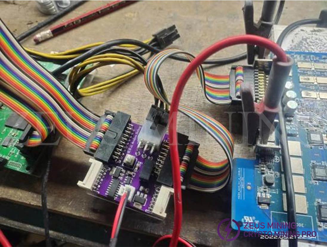
(8 ) Самодельный датчик короткого замыкания (используйте штифты для проводки и сварки, и необходимо нагреть термоусадочную втулку, чтобы предотвратить короткое замыкание между датчиком и небольшим радиатором).
5. Общие требования к запасным материалам для технического обслуживания:
Резистор 0402 (0Р, 51Р, 10К, 4,7К,);
Конденсатор 0402 (0,1мкФ, 1мкФ)
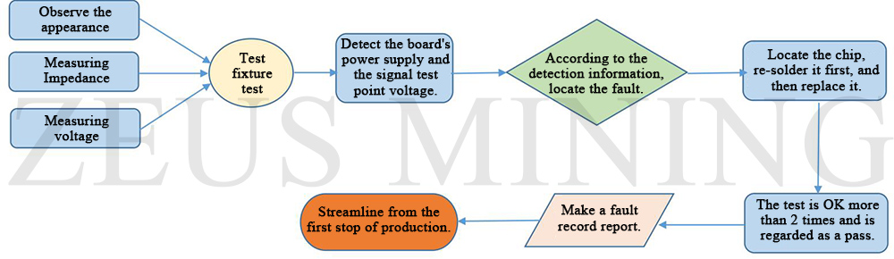
Ⅱ. Требования к техническому обслуживанию
1. Обратите внимание на метод работы при замене чипа. После замены каких-либо аксессуаров печатная плата не имеет явных деформаций. Проверьте запасные части и окружающие детали на отсутствие недостающих частей, обрывов цепи и коротких замыканий.2. Обслуживающий персонал должен обладать определенными знаниями в области электроники, иметь опыт обслуживания более одного года и владеть технологиями упаковки BGA/QFN/LGA и сварки.
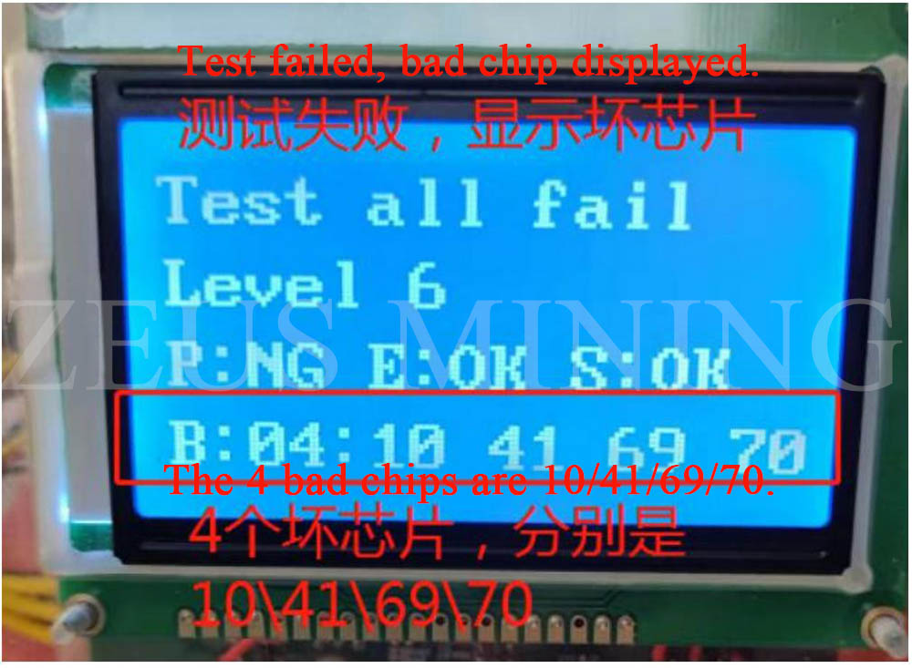
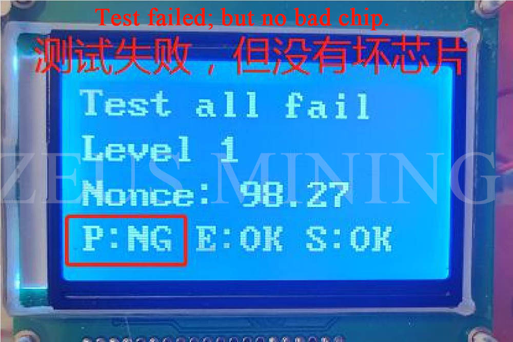
3. После ремонта хэш-доску необходимо протестировать более двух раз, и все в порядке!
4. Проверьте инструменты, может ли тестовое приспособление нормально работать, определите параметры тестового программного обеспечения станции технического обслуживания, версию тестового приспособления и т. д.
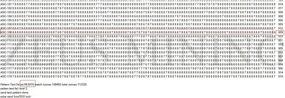
5. Для проверки ремонта и замены чипа необходимо сначала протестировать чип, а затем выполнить функциональный тест после прохождения. Функциональный тест должен убедиться, что малый радиатор приварен нормально, а большой радиатор установлен на место (каждый гель термоклея должен быть нанесен равномерно, а затем установлен большой радиатор), а охлаждающий вентилятор работает на полной скорости. При использовании шасси для отвода тепла следует размещать одновременно две хеш-панели, образующие воздуховод. Односторонний тест производства также должен гарантировать, что воздуховод сформирован (Важно)
6. При измерении сигнала помогите 4 вентиляторам рассеивать тепло, чтобы вентиляторы продолжали работать на полной скорости.
7. Когда хеш-плата включена, сначала должен быть подключен отрицательный медный провод источника питания, затем должен быть подключен положительный медный провод источника питания, и, наконец, должен быть вставлен сигнальный кабель. При разборке порядок установки должен быть обратным. Сначала отсоедините сигнальный кабель, затем отсоедините положительный медный провод источника питания и, наконец, отсоедините отрицательный медный провод источника питания. Если не соблюдать этот порядок, очень легко повредить U1 и U2 (не все фишки можно найти). Перед тестированием Pattern отремонтированная хеш-плата должна быть охлаждена перед тестированием, иначе это приведет к тестированию PNG.
8. Чтобы заменить новый чип, очистите контакты и припойную пасту, чтобы убедиться, что чип предварительно залужен, а затем припаян к печатной плате для ремонта.
9. Все тестовые приспособления на стороне обслуживания тестируются в режиме Test_Mode и в режиме кода сканирования. После прохождения теста производственная сторона будет оптимизирована с первой тестовой станции, а обычная установка будет устаревшей (установлена в соответствии с тем же уровнем).
Ⅲ. Производство испытательных приспособлений и меры предосторожности
Испытательное приспособление должно удовлетворять требованиям по рассеиванию тепла рабочей платой, чтобы облегчить измерение сигналов.1. Получите номер детали: испытательное приспособление ZJ0001000001.
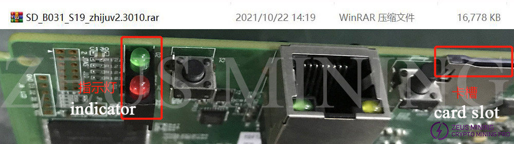
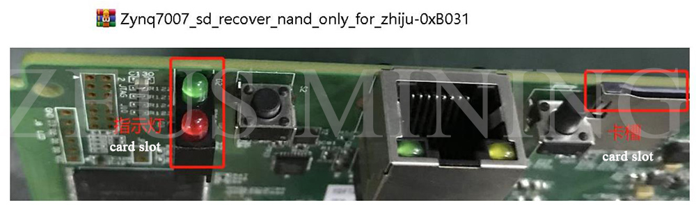
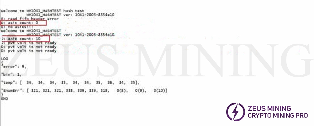
2. В первый раз используйте SD-карту тестового приспособления серии 19, чтобы провести программу для обновления FPGA платы управления тестовым приспособлением. После распаковки скопируйте его на SD-карту и вставьте карту в слот для карты тестового приспособления; подождите около 1 минуты после включения питания и подождите, пока индикатор платы управления не мигнет 3 раза дважды, это означает, что обновление завершено; (если он не обновлен, это может привести к тому, что определенный чип будет признан неисправным во время теста).
https://www.zeusbtc.com/share/antminer-d7-hash-board-repair-guide/indicator-light.jpg
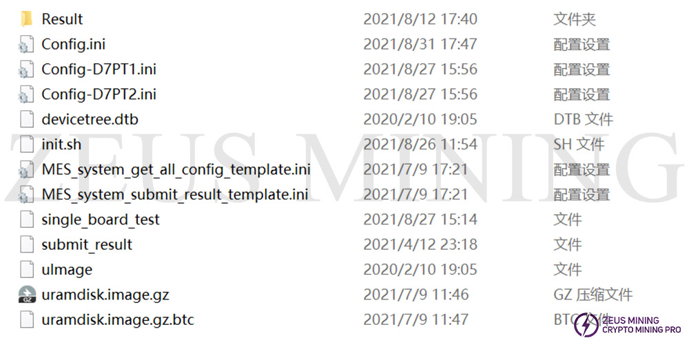
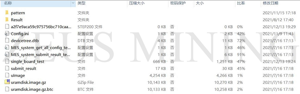
3. Сделайте тестовую SD-карту в соответствии с требованиями, односторонний радиатор обнаруживает чип и непосредственно распаковывает сжатый пакет, чтобы сделать SD-карту; PT1 не нужно сканировать код; версия программного обеспечения D7_PT1_test_zhiju_20210827. Скопируйте следующие файлы на SD-карту, производство завершено.
https://www.zeusbtc.com/share/antminer-d7-hash-board-repair-guide/pt1-software-file.jpg
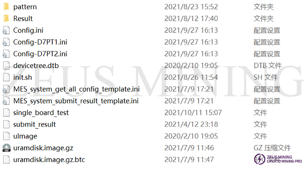
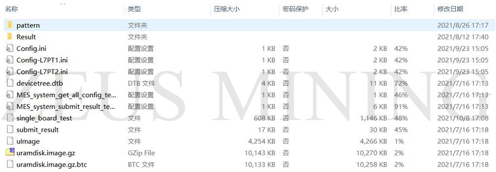
4. Сделайте тестовую SD-карту в соответствии с требованиями. Двухсторонний тест радиатора 8x Pattern должен сделать SD-карту, как показано на рисунке ниже; тест PT2 должен быть вставлен с кодовым пистолетом и сетевым кабелем. Версия программного обеспечения является версией программного обеспечения PT2, скопируйте следующее содержимое на SD-карту, чтобы завершить производство;
https://www.zeusbtc.com/share/antminer-d7-hash-board-repair-guide/pt2-software-file.jpg
5. При использовании двустороннего теста 8x Pattern на стороне производства, на стороне внутренних продаж и на стороне аутсорсингового обслуживания требуется соответствующий сканер кода и инструменты последовательного порта. Подробности см. в руководстве по тестированию D7.
Ⅳ. Обзор принципа
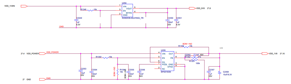
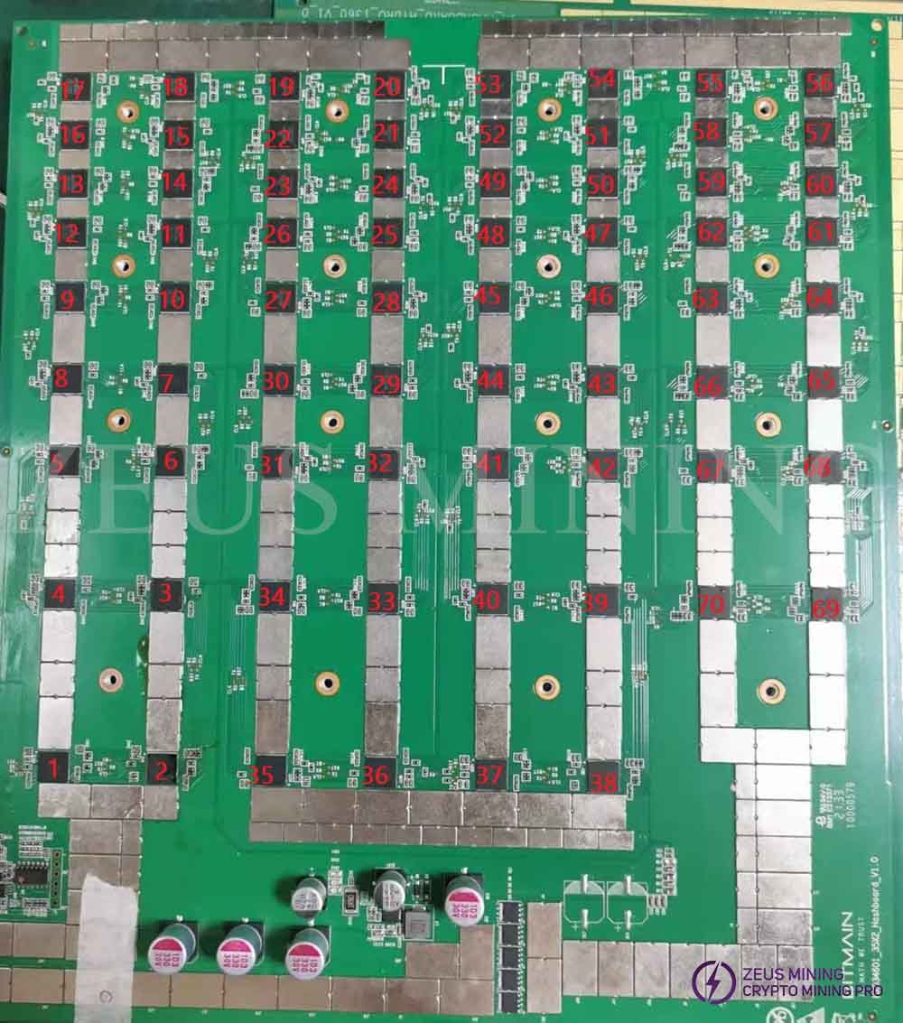
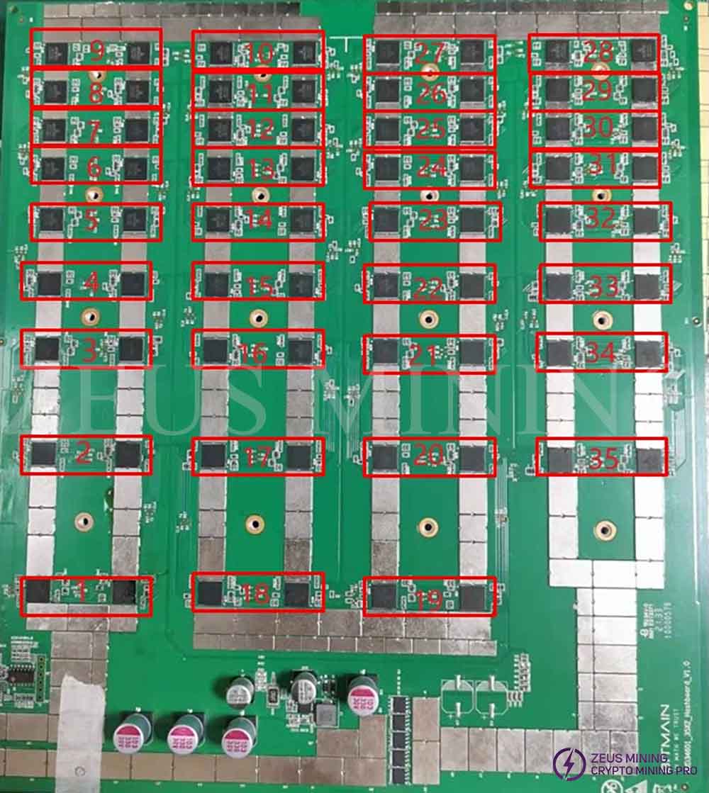
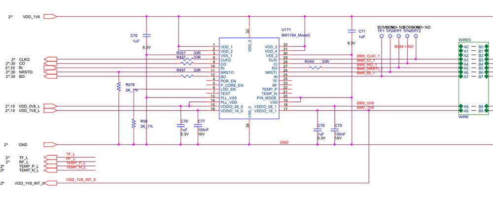
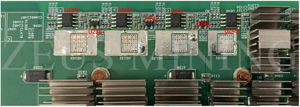
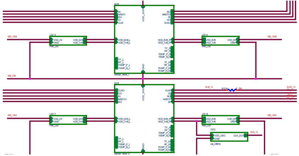
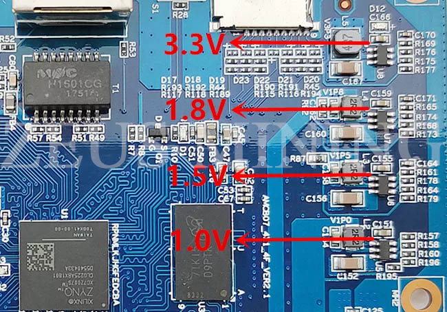
1. Рабочая структура хеш-платы D7:Хэш-плата D7 состоит из 70 чипов Antminer BM1764, которые разделены на 35 доменов, и каждый домен состоит из 2 чипов ASIC; рабочее напряжение микросхем BM1764, используемых в хеш-плате D7, составляет 0,3В; Выходное напряжение 20 В повышающей схемы U238 выводится линейным регулятором (U295 U16 U14 U307 U310 U313) для подачи 1,8 В на группы 29, 30, 31, 32, 33, 34 (всего 6 групп) для обеспечения LDO Источник питания 1,8 В, 1,8 В для LDO (U294 U15 U13 U306 U309 U312 U187 U188 U190 U191 U193 U194) выход 0,8 В. 28-я группа - 1-я группа и 35-я группа обеспечиваются VDD 13 В через LDO для обеспечения 1,8 В, 1,8 В, а затем через линейный регулятор для обеспечения 0,8 В, напряжение домена составляет около 0,3 В. Как показано на рисунке:
Группа 28 - Группа 1 и Группа 35
https://www.zeusbtc.com/share/antminer-d7-hash-board-repair-guide/domain-voltages-for-groups-1-and-35.jpg
Группы 29-34
https://www.zeusbtc.com/share/antminer-d7-hash-board-repair-guide/domain-voltages-for-groups-29-to-34.jpg
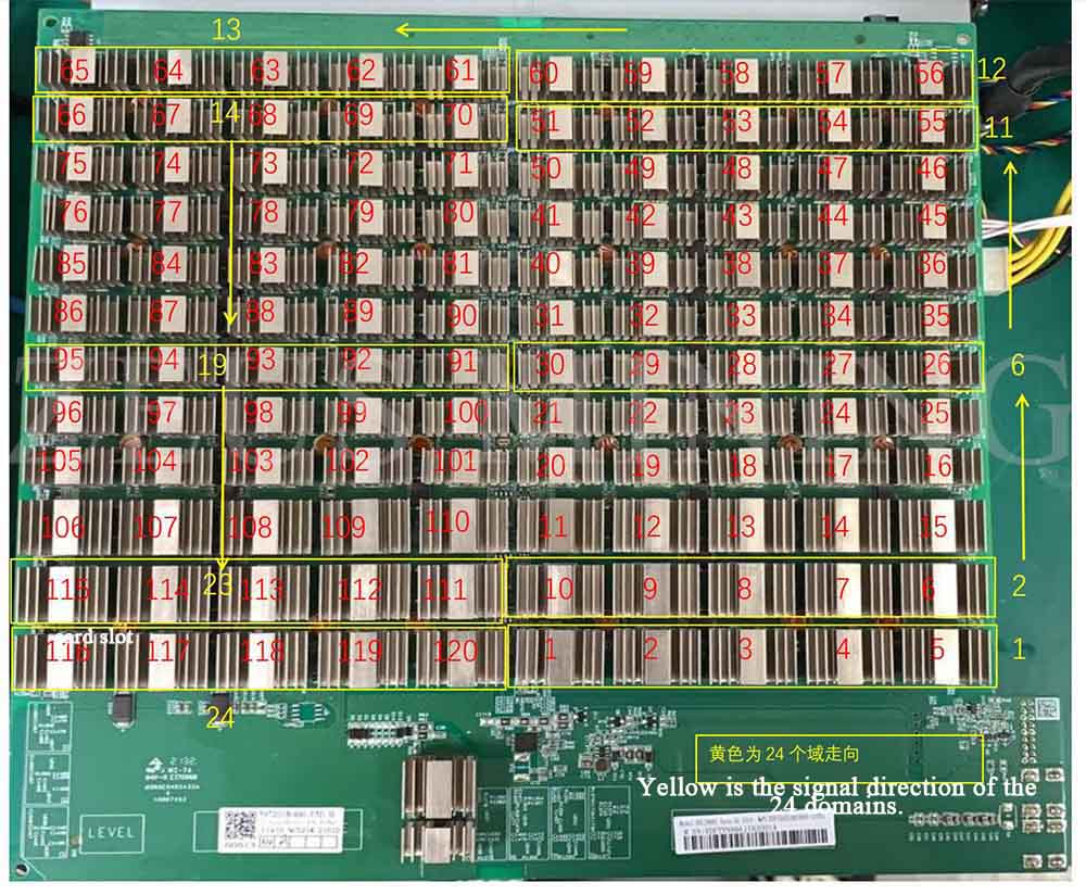
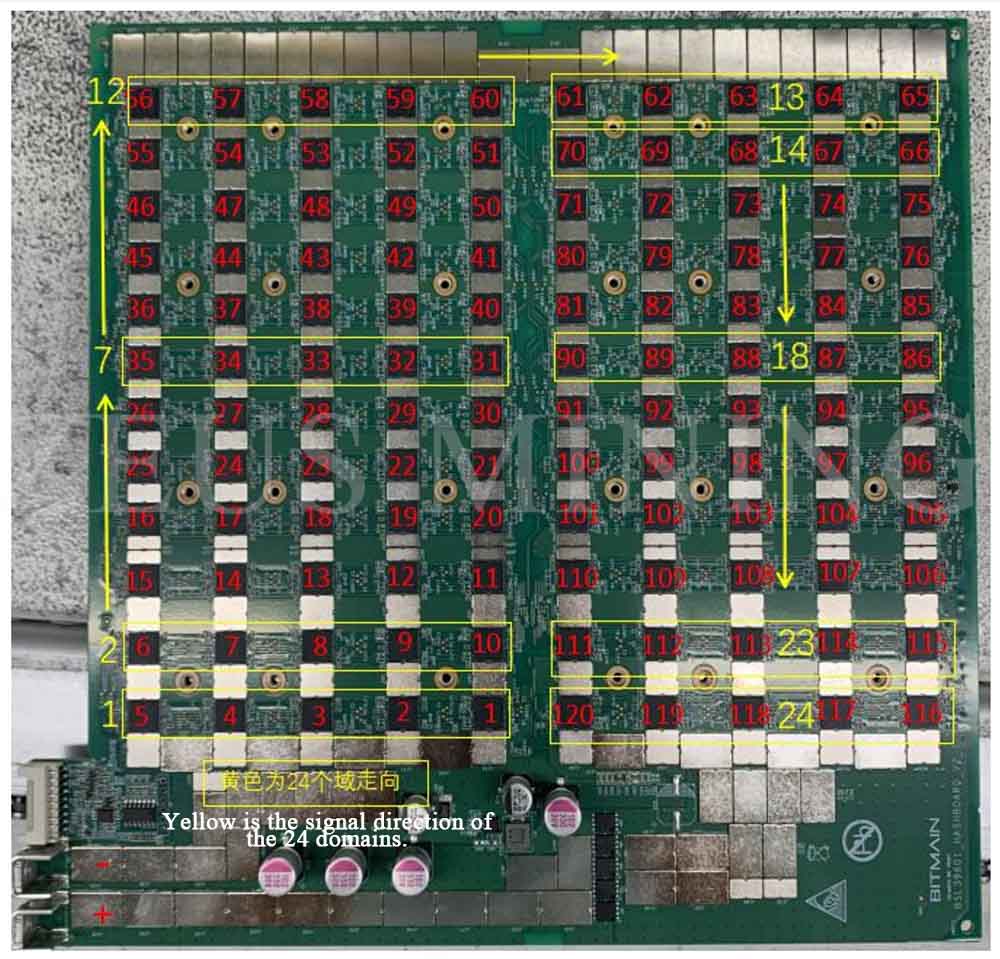
https://www.zeusbtc.com/share/antminer-d7-hash-board-repair-guide/d7-hash-board-chip-location.jpg
https://www.zeusbtc.com/share/antminer-d7-hash-board-repair-guide/d7-hash-board-voltage-domain.jpg
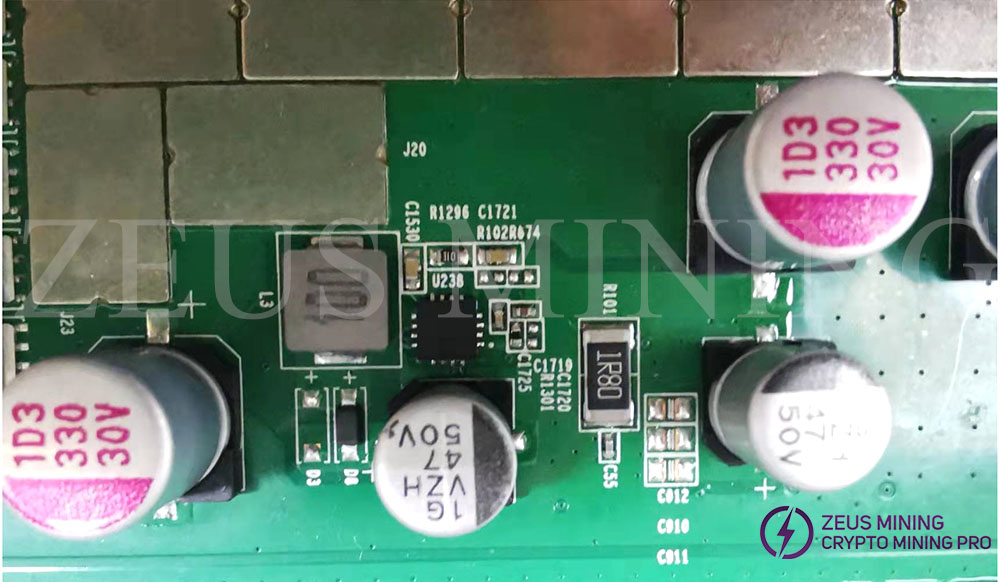
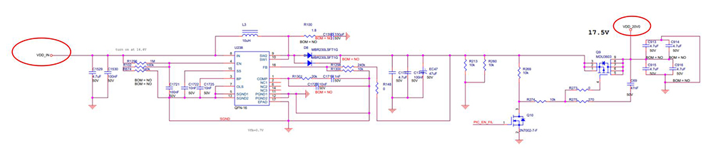
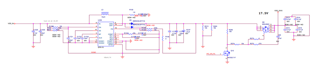
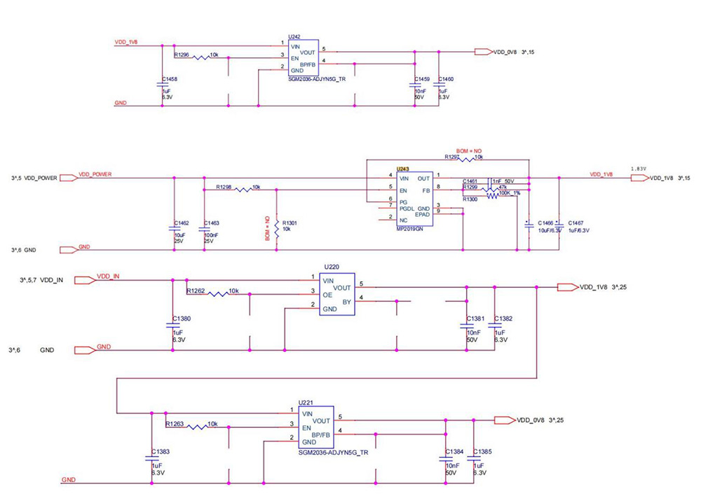
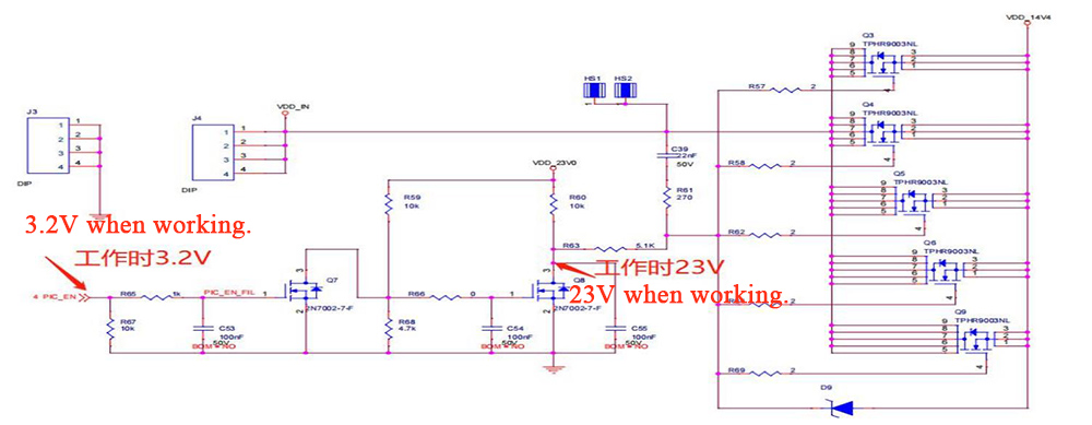
2. Схема повышения хеш-платы BXD34601:
Буст питается от 13В от блока питания и превращается в 20В, как показано на рисунке.
https://www.zeusbtc.com/share/antminer-d7-hash-board-repair-guide/d7-boost-circuit-location.jpg
https://www.zeusbtc.com/share/antminer-d7-hash-board-repair-guide/d7-boost-circuit-schematic.jpg
3. Направление сигнала чипа D7:
(1) Поток сигнала CLK (XIN) генерируется кварцевым генератором Y2 25 МГц и передается от чипа № 01 к чипу № 70; напряжение около 0,9В;
(2) Поток сигналов RST и CI поступает с 3-го контакта (3,3 В) J3 и преобразуется микросхемой преобразования уровней U1-U3-U4, а затем передается с микросхемы № 01 на микросхему № 70;
(3) Направление потока сигнала RX (RI, RO) от чипа № 70 к чипу № 01 и возвращается к контакту 8 разъема сигнального кабеля через U2, а затем возвращается к плате управления;
4) поток сигналов БО (БИ, ВО), от микросхемы № 01 к № 70;
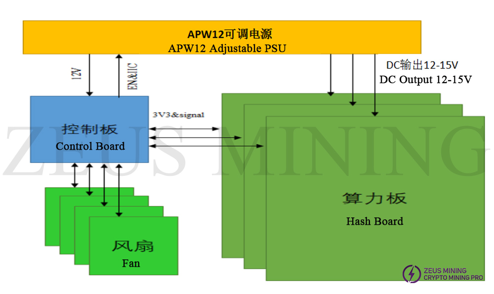
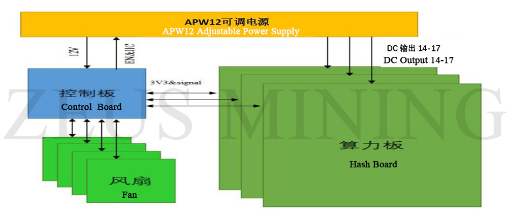
4. Вся структура майнера:
Весь майнер в основном состоит из 3 хеш-плат, 1 платы управления Antminer D7, блока питания APW12 и 4 охлаждающих вентиляторов, как показано на рисунке:
https://www.zeusbtc.com/share/antminer-d7-hash-board-repair-guide/d7-miner-architecture.jpg
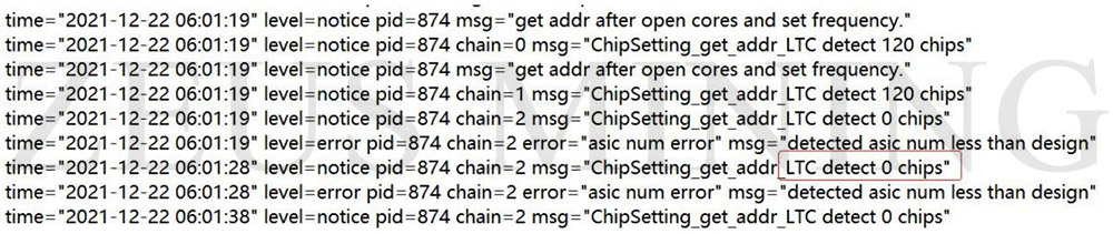
Ⅴ. Распространенные проблемы и шаги по устранению неполадок с хэш-доской
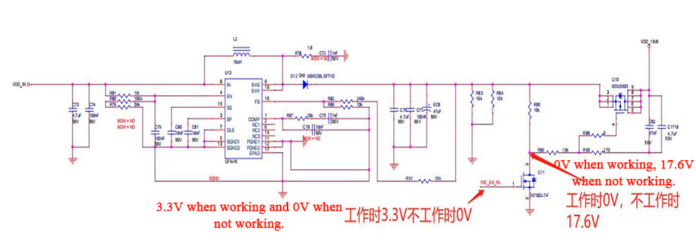
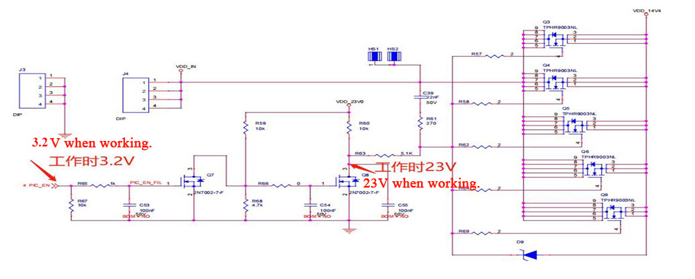
Явление 1: тест одной платы обнаруживает, что чип равен 0 (станция PT1/PT2)Первый шаг: сначала проверьте выходную мощность, пожалуйста, проверьте напряжение в обведенной части на рисунке ниже.
https://www.zeusbtc.com/share/antminer-d7-hash-board-repair-guide/power-output-schematic.jpg
https://www.zeusbtc.com/share/antminer-d7-hash-board-repair-guide/check-the-circle-area-voltage.jpg
Второй шаг: проверьте выходное напряжение домена напряжения
Напряжение каждого домена напряжения составляет около 0,3 В, а источник питания 13 В обычно имеет напряжение домена. Приоритет отдается измерению выходного сигнала клеммы питания хеш-платы, а также проверке наличия короткого замыкания МОП (измерьте сопротивление резистора между контактами 1, 4 и 8 ). Если питание 13В есть, но напряжения домена нет, продолжайте проверку.
https://www.zeusbtc.com/share/antminer-d7-hash-board-repair-guide/mos-chip-location.jpg
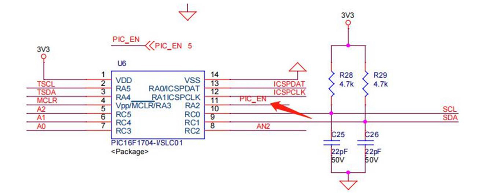
Третий шаг: проверьте цепь PIC
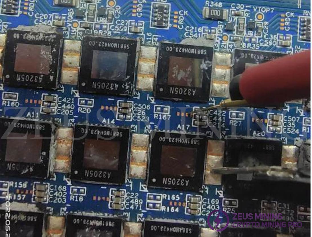
Измерьте, имеет ли контакт 11 U6 выход (3,3 В). Если да, продолжайте устранять проблему. Если нет, убедитесь, что соединение между кабелем тестового приспособления и хэш-платой в порядке, и перепрограммируйте PIC.
https://www.zeusbtc.com/share/antminer-d7-hash-board-repair-guide/pic-circuit-schematic.jpg
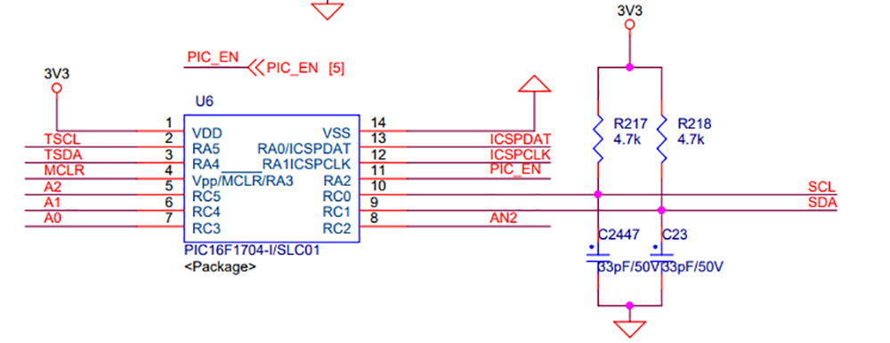
https://www.zeusbtc.com/share/antminer-d7-hash-board-repair-guide/pic-location.jpg
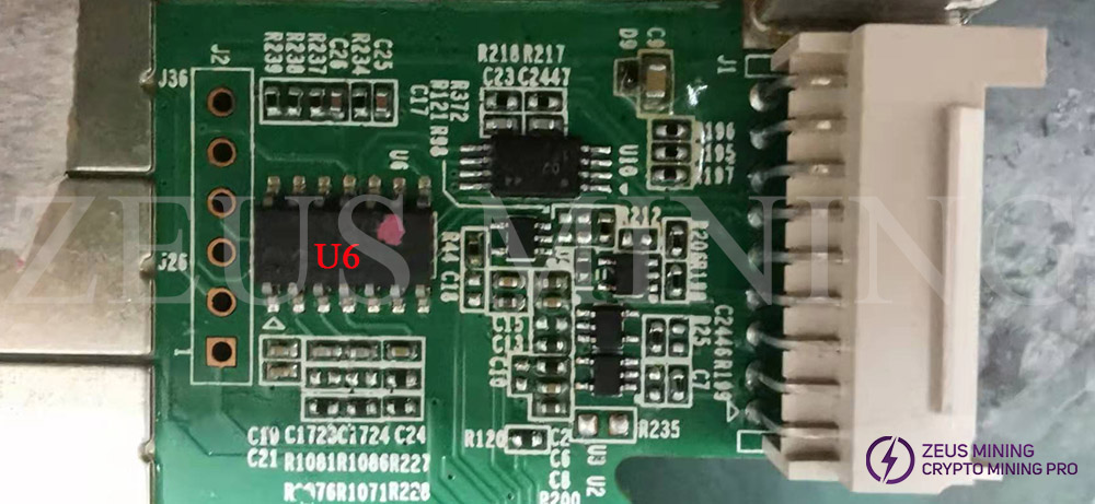
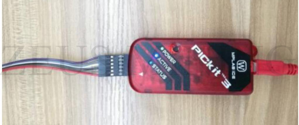
Шаги программирования PIC:
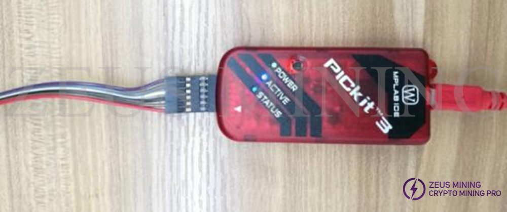
(1) Запишите программу PIC хеш-платы.
Загрузите инструмент программирования: программатор PICkit3.5, контакт 1 кабеля PICkit3 соответствует контакту 1 J3 на печатной плате и должен быть подключен к контактам 1, 2, 3, 4, 5 и 6.
https://www.zeusbtc.com/share/antminer-d7-hash-board-repair-guide/pickit3-programming-tool.jpg
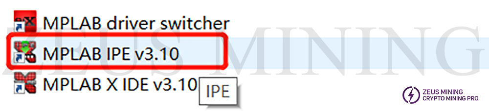
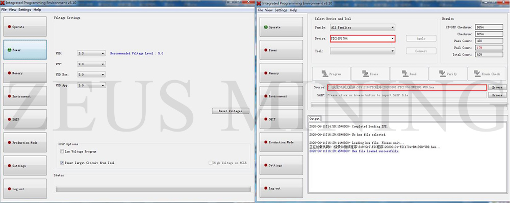
(2) Программное обеспечение для записи:
① Откройте MPLAB IPE, выберите устройство: PIC16F1704;
② Нажмите «Power», чтобы выбрать способ подачи питания, а затем нажмите «Operate»;
③ Выберите file, чтобы найти файл .HEX для записи;
④ Нажмите «connect», подключение нормальное.
⑤ Нажмите кнопку «Program».
⑥ После завершения нажмите «Verifiy», чтобы подтвердить успешность записи.
https://www.zeusbtc.com/share/antminer-d7-hash-board-repair-guide/mplab-ipe-software.jpg
https://www.zeusbtc.com/share/antminer-d7-hash-board-repair-guide/mplab-ipe-running-interface.jpg
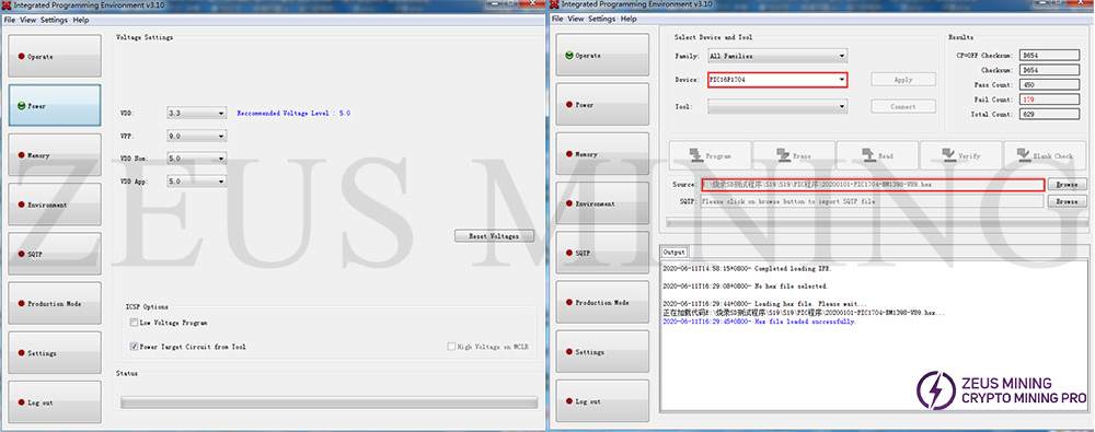
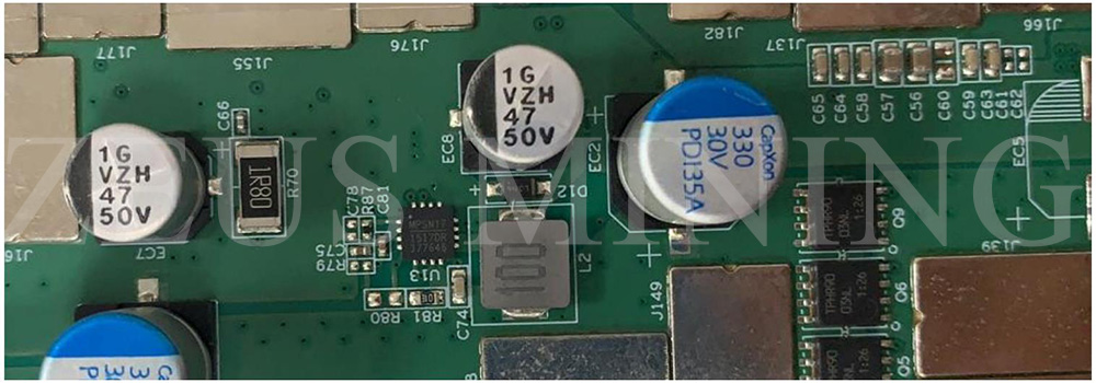
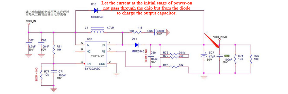
Четвертый шаг: проверьте выход схемы усилителя и проверьте C69 на следующем рисунке, и напряжение может быть измерено до 20 В.
https://www.zeusbtc.com/share/antminer-d7-hash-board-repair-guide/measured-to-boost-circuit-20v-voltage.jpg
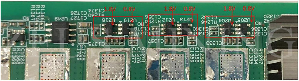
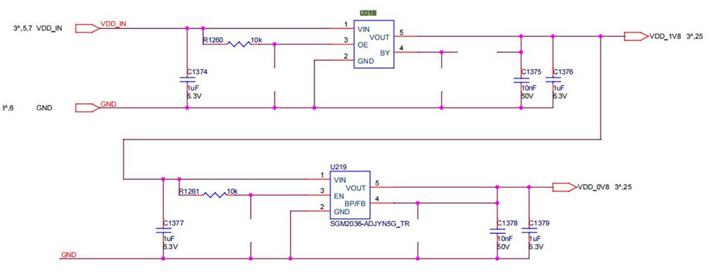
Пятый шаг: проверьте каждую группу выхода LDO 1,8 В или PLL 0,8 В.
Группа 28 - Группа 1 и Группа 35
https://www.zeusbtc.com/share/antminer-d7-hash-board-repair-guide/group-28-ldo-and-pll-voltage-outputs.jpg
Группы 29-34
https://www.zeusbtc.com/share/antminer-d7-hash-board-repair-guide/groups-29-34-ldo-and-pll-voltage-outputs.jpg
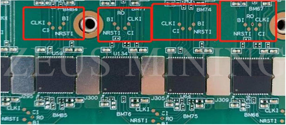
Шестой шаг: проверьте вывод сигнала чипа (CLK/CI/RO/BI/RST)
Диапазон значений напряжения описывается направлением опорного сигнала. Если при измерении обнаруживается большое отклонение значения напряжения, его можно сравнить со значением измерения соседней группы.
https://www.zeusbtc.com/share/antminer-d7-hash-board-repair-guide/chip-test-point-signal-schematic.jpg
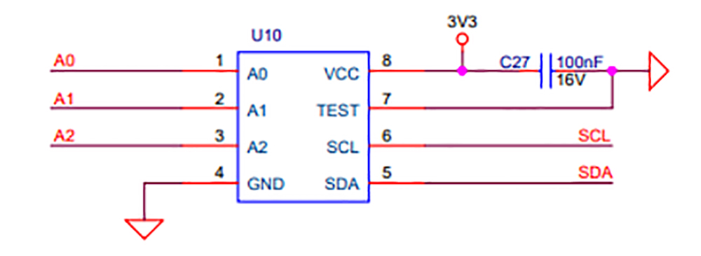
Когда на ЖК-экране тестового приспособления отображается EEPROM NG, проверьте, нормально ли припаян U10;
https://www.zeusbtc.com/share/antminer-d7-hash-board-repair-guide/u10-voltage-schematic.jpg
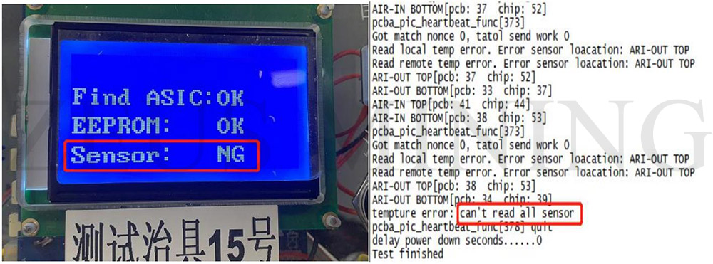
Когда датчик PIC NG отображается на ЖК-экране тестового приспособления, температура показаний теста не соответствует норме. Для устранения неполадок выполните следующие действия:
а) Проверьте, н