DeathAndTaxes (OP)
Donator
Legendary

 Offline Offline
Activity: 1218
Merit: 1079
Gerald Davis

|
 |
January 27, 2012, 01:42:04 PM |
|
So AMD graphic cards use seperate VRM for memory voltage. The 5970 for example runs at 1.05V core and 1.10V memory stock.
All this talk of undervolting got me thinking. 2GB of RAM uses some wattage. We are underclocking the memory 50% to 80% or more it likely can run stable at much lower voltage. None of the tools I have seen allows the voltage to be adjusted DOWNWARD.
XFX Black Edition has a tool which allows memory voltage to be increased independently of core by up to 15% so modification is physically possible. I guess XFX never though people would want to underclock the memory.
Any ideas? Has anyone tried?
|
|
|
|
|
|
|
|
Be very wary of relying on JavaScript for security on crypto sites. The site can change the JavaScript at any time unless you take unusual precautions, and browsers are not generally known for their airtight security.
|
|
|
Advertised sites are not endorsed by the Bitcoin Forum. They may be unsafe, untrustworthy, or illegal in your jurisdiction.
|
|
|
|
|
|
bulanula
|
|
January 27, 2012, 02:03:46 PM |
|
So AMD graphic cards use seperate VRM for memory voltage. The 5970 for example runs at 1.05V core and 1.10V memory stock.
All this talk of undervolting got me thinking. 2GB of RAM uses some wattage. We are underclocking the memory 50% to 80% or more it likely can run stable at much lower voltage. None of the tools I have seen allows the voltage to be adjusted DOWNWARD.
XFX Black Edition has a tool which allows memory voltage to be increased independently of core by up to 15% so modification is physically possible. I guess XFX never though people would want to underclock the memory.
Any ideas? Has anyone tried?
Good idea ! I am also wondering if this VRM on the left in this picture is the VRM in question and this is the one that is powering the memory modules in question on a reference 5870 :  For anyone that does not know that VRM supposedly is only used for the memory of the card and it is located between the leftmost memory chip and the capacitor on the left side ! |
|
|
|
|
DeathAndTaxes (OP)
Donator
Legendary
Offline
Activity: 1218
Merit: 1079
Gerald Davis
|
|
January 27, 2012, 02:17:33 PM |
|
Is that a 5870 PCB but it doesn't look "right" for a 5970? Still I am 99% sure regardless of where it physically is located all AMD card use a different bank of VRMs for memory voltage because they run at a different voltage.
|
|
|
|
|
|
bulanula
|
|
January 27, 2012, 02:20:40 PM |
|
Is that a 5870 PCB but it doesn't look "right" for a 5970? Still I am 99% sure regardless of where it physically is located all AMD card use a different bank of VRMs for memory voltage because they run at a different voltage.
Actually that is a picture from a reference 5850 card I found on the net and edited myself to show the VRM location. I have checked on one of my 5870 that the VRM is also there on the reference 5870s. I have no 5970s so I cannot check first hand. |
|
|
|
|
DeathAndTaxes (OP)
Donator
Legendary
Offline
Activity: 1218
Merit: 1079
Gerald Davis
|
|
January 27, 2012, 02:40:38 PM |
|
A little more VRM pr0n. 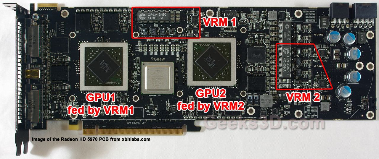 The rectangle "big" chip at the top marked CPLA-3-50 is commonly incorrectly called the VRM. It isn't. It is an inductor. The amperage used by GPU mean an external inductor is necessary. The "A" =low acoustic noise model. 3 = 3 phase. 50=peak amperage (rated for 40). The 3 small chips directly below the CPLA-3-50 are the VRMs. The 5970 uses 3 phase power. The actual GPU (the chip not the card) was designed to be powered by 4 phase power. The 5970s are downclocked 5870s and AMD realized 3 phase is sufficient. You will notice the board was designed for a 4th VRM. Saves about $12 per board using 3 phase instead of 4 phase power.  The square chip to the right (next the to red "V") is the controller for the VRM array. It can alter the voltage between 0.6V and 2.0V (doesn't mean GPU can handle that). It also handles thermal throttling (idles card for some % of clock cycles if VRM temps get over 120C). On 5970 each GPU subsystem is completely independent. It is basically 2 entire cards sandwiched together and connected to a PCIe switch (big chip in dead center between the two GPUs). Each GPU acts as if it is an independent card (w/ exception of fan control but even that is hidden from GPU). Lastly the CP-2-50 is the inductor for non-GPU (AMD calls it "uncore") VRMs. Yeah AMD decided to skip low acoustic noise version. Saves about $0.20 in bulk. I believe this array (2 VRM, 1 controller, 1 inductor) drives the mem voltage. Technically called VDCCI for I/O. One possible warning. IIRC all non-GPU voltage are handled by this "memory VRM". A very low voltage could cause other components like PCIe switch, fan controller, monitoring ASIC, etc to fail (hopefully soft failure). One should be careful and conservative in lowering the VDDCI voltage because it doesn't power just the memory. Here is a shot of 5870. You notice similar configuration except 4 phase power for those power hungry top-clocked 5870s. You should see 1 4 phase inductor, 4 VRMs, 1 controller. |
|
|
|
|
DeathAndTaxes (OP)
Donator
Legendary
Offline
Activity: 1218
Merit: 1079
Gerald Davis
|
|
January 27, 2012, 02:43:19 PM |
|
Is that a 5870 PCB but it doesn't look "right" for a 5970? Still I am 99% sure regardless of where it physically is located all AMD card use a different bank of VRMs for memory voltage because they run at a different voltage.
Actually that is a picture from a reference 5850 card I found on the net and edited myself to show the VRM location. I have checked on one of my 5870 that the VRM is also there on the reference 5870s. It is possible but if it there is only 1 VRM = 1 phase power w/ no external inductor. I doubt that would be sufficient to power the memory. On 5850 maybe but 5870s have up to 1GB of memory clocked very high. I would imagine it needs a beefier setup. See above for my theory on VDDC system for 5970. I will look at 5870 PCB and see if there are any other alternatives. On edit: Take a look at these shots of 5870   Notice that massive cooler doesn't cover the chip in upper left. It would be "weird" (but not impossible) for an aftermarket cooler to not cool the memory VRM as you would just move the bottleneck from GPU to memory. |
|
|
|
|
|
bulanula
|
|
January 27, 2012, 02:48:08 PM |
|
Is that a 5870 PCB but it doesn't look "right" for a 5970? Still I am 99% sure regardless of where it physically is located all AMD card use a different bank of VRMs for memory voltage because they run at a different voltage.
Actually that is a picture from a reference 5850 card I found on the net and edited myself to show the VRM location. I have checked on one of my 5870 that the VRM is also there on the reference 5870s. It is possible but if it there is only 1 VRM = 1 phase power w/ no external inductor. I doubt that would be sufficient to power the memory. On 5850 maybe but 5870s have up to 1GB of memory clocked very high. I would imagine it needs a beefier setup. See above for my theory on VDDC system for 5970. I will look at 5870 PCB and see if there are any other alternatives. Yes I am very interested what that left single VRM does but as far as I can see there is no inductor but there is another one of those Volterra controllers ( 2 in total for a 5870 ) along the single VRM next to the memory chips. |
|
|
|
|
DeathAndTaxes (OP)
Donator
Legendary
Offline
Activity: 1218
Merit: 1079
Gerald Davis
|
|
January 27, 2012, 02:53:48 PM
Last edit: January 27, 2012, 03:24:15 PM by DeathAndTaxes |
|
Yes I am very interested what that left single VRM does but as far as I can see there is no inductor but there is another one of those Volterra controllers ( 2 in total for a 5870 ) along the single VRM next to the memory chips.
You could be right. Maybe my assumption is wrong. Maybe memory doesn't pull that much amperage and thus doesn't need any serious cooling. If you look back at the 5970 it has the same single VRM, no inductor, and controller group right under the word "VRM 1". [slightly off topic] It is a mystery. I wish AMD gave detailed technical specs. I guess you need to be a Tier 1 partner and sign an NDA. I wonder if someone got enough capital if you could make a mining card based on AMD GPU. Make it 1x PCIe slot, 2 or 3 GPUs, minimal memory, and massively beefed up VRM system. I wonder if AMD would authorize something like that. Hell you wouldn't have to call it a Bitcoin miner you could call it a GPGPU device (like Tesla). Maybe get AMD low bin chips and underclock them to improve MH/W. I think w/ a slimed down board, a 7800 series GPU and minimal memory you could get 7 or maybe 8 MH/W. I would give FPGA a run for their money. Hell it is almost as efficient as BFL's toaster. [/slightly off topic] |
|
|
|
|
|
bulanula
|
|
January 27, 2012, 03:07:38 PM |
|
It would be "weird" (but not impossible) for an aftermarket cooler to not cool the memory VRM as you would just move the bottleneck from GPU to memory. Yes that is clearly a design error by the aftermarket cooler producer. Check this heatsink ( little red on on the left ) made specifically to cover that memory VRM on the 5870 and the nearest memory chip !  Picture of the VRM locations on a reference 5870 PCB  |
|
|
|
|
DeathAndTaxes (OP)
Donator
Legendary
Offline
Activity: 1218
Merit: 1079
Gerald Davis
|
|
January 27, 2012, 03:28:16 PM |
|
Well that last image is interesting.
5870 uses 4 phase power for GPU. Look to the right of the inductor. You got 4 VRMs there. It is unclear when the 5th component in the red box (from the bottom) is but the next two look like another pair of VRMs. The 5970 has a pair of VRMs in that location too. Wonder that they are used for?
If someone had a IR thermometers you could find out real easy. Measure the VRM in upper left and upper right at idle and max memory overclock running something like furmark. One should get much hotter than the other and that is likely the VRM handling memory voltage.
|
|
|
|
|
DeathAndTaxes (OP)
Donator
Legendary
Offline
Activity: 1218
Merit: 1079
Gerald Davis
|
|
January 27, 2012, 03:29:50 PM
Last edit: January 27, 2012, 03:50:14 PM by DeathAndTaxes |
|
Back to the original question. I did some googling and the only way I found to lower the memory (not core) voltage is via BIOS flash. I may experiment this weekend.
|
|
|
|
|
rjk
Sr. Member
 Offline
Activity: 448
Merit: 250
1ngldh
|
|
January 27, 2012, 03:33:03 PM |
|
Picture of the VRM locations on a reference 5870 PCB It appears that there are four VRMs starting from the bottom of the picture, followed by one blank spot for a fifth VRM. Above those, are two other VRMs, and my hypothesis is that they are for the memory. EDIT: My hypothesis for the one in the top left is that it runs an HDMI/DisplayPort switch, or some other auxiliary electronics. |
|
|
|
|
ArtForz
|
|
January 27, 2012, 06:46:35 PM |
|
A little more VRM pr0n. If you look closely, you'll find several more VRMs on the 5970 first the obvious ones: VRM1 area = VT1165 + 3 slaves, GPU1 VDDC (i2c slave addr 0x70 on gpu1) VRM2 area = VT1165 + 3 slaves, GPU2 VDDC (i2c slave addr 0x70 on gpu2) the square chip at the top/right of vrm2 area = another vt1165 controller, belongs to the 2 slaves above the VRM2 slaves, it's a 2-phase providing both GPUs VDDCI (i2c slave addr 0x71 on gpu1) now, there's avolterra integrated controller (vt237) top/right of the 1 of "VRM1" and another vt237 under the R of "VRM2" I suspect those 2 guys are our memory VCC (one for each GPUs memory?). now on to the non-volterra stuff a AOZ1024D above the VDDCI inductors and output caps... no clue. the 2 FETs below the GPU2 memory chips/left of the suspected GPU2 memory VRM, controller is a uP6101 on the backside ... again, random aux supply. that should be it for major switchers, there's probably another 3 or 4 linear regs strewn about... |
bitcoin: 1Fb77Xq5ePFER8GtKRn2KDbDTVpJKfKmpz
i0coin: jNdvyvd6v6gV3kVJLD7HsB5ZwHyHwAkfdw
|
|
|
|
bulanula
|
|
January 27, 2012, 07:49:49 PM |
|
A little more VRM pr0n. If you look closely, you'll find several more VRMs on the 5970 first the obvious ones: VRM1 area = VT1165 + 3 slaves, GPU1 VDDC (i2c slave addr 0x70 on gpu1) VRM2 area = VT1165 + 3 slaves, GPU2 VDDC (i2c slave addr 0x70 on gpu2) the square chip at the top/right of vrm2 area = another vt1165 controller, belongs to the 2 slaves above the VRM2 slaves, it's a 2-phase providing both GPUs VDDCI (i2c slave addr 0x71 on gpu1) now, there's avolterra integrated controller (vt237) top/right of the 1 of "VRM1" and another vt237 under the R of "VRM2" I suspect those 2 guys are our memory VCC (one for each GPUs memory?). now on to the non-volterra stuff a AOZ1024D above the VDDCI inductors and output caps... no clue. the 2 FETs below the GPU2 memory chips/left of the suspected GPU2 memory VRM, controller is a uP6101 on the backside ... again, random aux supply. that should be it for major switchers, there's probably another 3 or 4 linear regs strewn about... What about the leftmost VRM on the 5870s ? What is that used for ? What about the 2 smaller VRMs on the right side above ? What about the 4 bigger VRMs near the inductor thingy ? Thanks ! |
|
|
|
|
|
ArtForz
|
|
January 27, 2012, 08:47:30 PM
Last edit: January 27, 2012, 08:59:07 PM by ArtForz |
|
on ref 5870 that VRM slave with a missing brother in the top left is the VDDCI, its vt1165 controller is in the extreme top left corner. memory VDD is the 2 above the missing 5th VDDC phase on the right (looks like those 2 are actually set up to run as a 2-phase... hard to tell from tiny pics) on nonrefs... well, anything can be anywhere  edit: nope, those 2 are 2 single vt243s, most likely memory VDDC and VDDQ |
bitcoin: 1Fb77Xq5ePFER8GtKRn2KDbDTVpJKfKmpz
i0coin: jNdvyvd6v6gV3kVJLD7HsB5ZwHyHwAkfdw
|
|
|
|
bulanula
|
|
January 28, 2012, 10:22:40 AM |
|
on ref 5870 that VRM slave with a missing brother in the top left is the VDDCI, its vt1165 controller is in the extreme top left corner. memory VDD is the 2 above the missing 5th VDDC phase on the right (looks like those 2 are actually set up to run as a 2-phase... hard to tell from tiny pics) on nonrefs... well, anything can be anywhere edit: nope, those 2 are 2 single vt243s, most likely memory VDDC and VDDQ Yes I am interested in this VRM. What does it do exactly ? |
|
|
|
|
|
Brunic
|
|
January 28, 2012, 08:19:51 PM |
|
Really interesting topic guys, I'll follow that.
|
|
|
|
|
|
ArtForz
|
|
January 28, 2012, 11:30:25 PM |
|
on ref 5870 that VRM slave with a missing brother in the top left is the VDDCI, its vt1165 controller is in the extreme top left corner. memory VDD is the 2 above the missing 5th VDDC phase on the right (looks like those 2 are actually set up to run as a 2-phase... hard to tell from tiny pics) on nonrefs... well, anything can be anywhere edit: nope, those 2 are 2 single vt243s, most likely memory VDDC and VDDQ Yes I am interested in this VRM. What does it do exactly ? It's the VDDCI VRM. it does VDDCI  Seriously, VDDCI = "uncore" ... as far as I can tell it's PCIe and memory controller core voltage. |
bitcoin: 1Fb77Xq5ePFER8GtKRn2KDbDTVpJKfKmpz
i0coin: jNdvyvd6v6gV3kVJLD7HsB5ZwHyHwAkfdw
|
|
|
|
SlaveInDebt
|
|
January 29, 2012, 02:51:27 AM |
|
5970/5850 3 phase, 5870 4 phase gpu. The memory phase is located above the gpu phase on 5870. You can undervolt the memory controller using GPUTool. .95v is idle default.  |
"A banker is a fellow who lends you his umbrella when the sun is shining, but wants it back the minute it begins to rain." - Mark Twain
|
|
|
DeathAndTaxes (OP)
Donator
Legendary
Offline
Activity: 1218
Merit: 1079
Gerald Davis
|
|
January 29, 2012, 03:03:52 AM |
|
5970/5850 3 phase, 5870 4 phase gpu. The memory phase is located above the gpu phase on 5870. You can undervolt the memory controller using GPUTool. .95v is idle default. Nice. I will check that out for my workstation. The bad news is my other 4 rigs are linux and GPUTool doesn't support Linux.  |
|
|
|
|
|


