|
velacreations
|
 |
September 14, 2013, 11:03:46 PM |
|
Yes and no. Labcoin is not 100 % consistent which was the initial spark that triggert the recent sell-off. But since then it was fueled by more than 1000 posts of less than 15 users. (estimated)
I for one am sure that they are real and the update/pictures from yesterday showed that they are working on it. You can argue about the price, you can argue about the timeline and you can argue about the PR style, that's personal risk each one has to take for himself.
really? you're gonna blame the crash on the shareholders, and not the guys that totally dropped the ball on the "announcement" and failed to provide any tangible evidence that anything they said is true? What about all the broken promises, like photos before the 10th, locking of shares, hash rate on the website, photos of the mining operation, etc, etc, etc? nah, it's the fault of people on the forum, not the guys that were begging people to buy shares!  |
|
|
|
|
|
|
Once a transaction has 6 confirmations, it is extremely unlikely that an attacker without at least 50% of the network's computation power would be able to reverse it.
|
|
|
Advertised sites are not endorsed by the Bitcoin Forum. They may be unsafe, untrustworthy, or illegal in your jurisdiction.
|
|
Ytterbium
|
|
September 14, 2013, 11:14:44 PM
Last edit: September 14, 2013, 11:28:33 PM by Ytterbium |
|
 All I see here in these pictures (both) are a single faced PCB, with no visible core vias, a grid of chip pads and what seems to be a bigger SMD pad like a capacitor or resistor. Only the SMD component seems to have visible vias which go and fill completely the connection pads at the end of the board. So the chip pads don't seem to connect to anything, and there is only one side shown in both pictures. OMG, are you calling the traces on the top layer of the PCB the "Vias"? Vias are connections between layers Like this:  The vias are underneath the pads and would connect the chips to wires on other layers of the PCBLook at the bitfury H-board  There are only traces on one of the four sides of the chip. According to your "analysis" that would mean only one side of the chip is connected to anything, and it's only connected to back to itself as well. That's not how circuit boards work. There are vias that connect the multiple layers of the circut board. You can't see the vias if they are underneath the SMD pads. There are likely vias underneath the pads for the chip. I agree that Labcoin has done a bad job communicating and is probably having lots of technical problems.
And it's completely ridiculous for them to not post more photos. However, claiming that the PCBs aren't connected is just completely ignorant of what real circuit boards actually look like. It's completely ridiculous nonsense. You're even using the terminology completely incorrectly. The flat lines on layers of the board are traces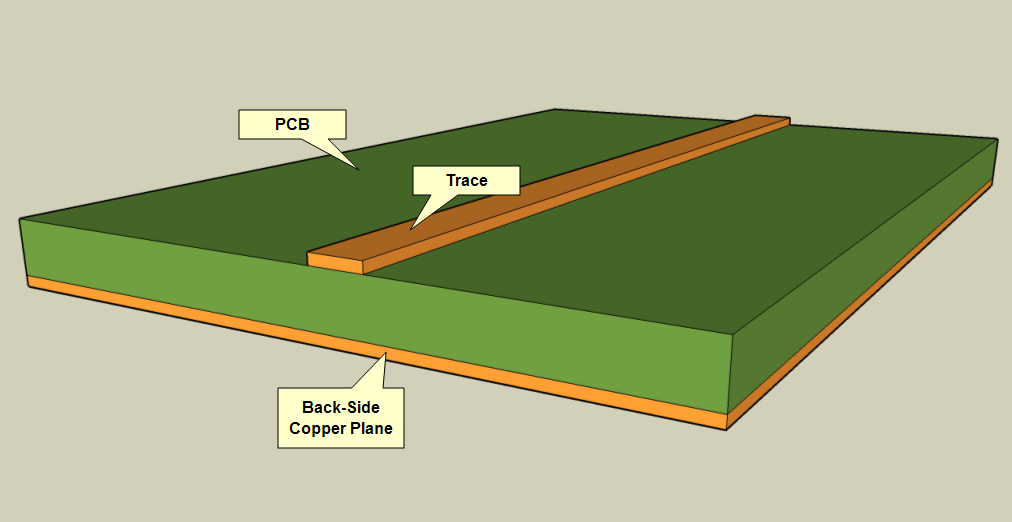 Vais are links between layers:   Completely ridiculous. Also, with the number of pins, chips typically have way more internal pads then external pins. The Avalon chip has far more pads then external pins. The reason is, most of those pads are just for power, not signals, and they are connected to the same external leads. |
|
|
|
dexX7
Legendary

 Offline Offline
Activity: 1106
Merit: 1024


|
|
September 14, 2013, 11:15:58 PM |
|
The boards they showed don't even have traces for the chips. How do you explain that?
Meh, sorry. What does "traces" mean in this context? Circuit paths? I'm not that deep into this topic, but maybe they are on the other side? Maybe the board manufactor even screwed up and some layers were not "printed". I have no idea. As far as I know they are in an experimental stage right now and I wouldn't wonder, if they do the tests on breadboards anyway, because they also said they aren't at a productional level yet. Edit: Ytterbium seems to know more about this.But as said before, there are some things that seem strange, but I also think the current price reflects that. Thus it comes down to the "is it a full blown scam or or" question and I'm clearly in for the later. Right now people are expecting "something" and Labcoin tries to deliver "something", but it clearly doesn't work to a satisfying degree and the number of angry posters as well as rushed answers from Labcoin shows that. Edit: really? you're gonna blame the crash on the shareholders, and not the guys that totally dropped the ball on the "announcement"
No, of course not. As said before "initiated by Labcoin, fueled by posters", dispite that, there was a huge level of tape painting involved. |
|
|
|
|
Ytterbium
|
|
September 14, 2013, 11:35:25 PM |
|
We are here to stay and everyone who is having doubts will have to change his opinion once we show what we achieved.
Again, we advise anyone to purchase more shares now that they are cheap.
Do you still confirm that these two pictures represent reality?   If so, please explain how the number of pins is different (128 vs 44) between the design and the boards/tray. You may also explain how the "giggahashes" send the results to the internet through the resistor/capacitor pin (which seems to be the only one thing connectable on the board). Or perhaps you might think this board filled with hardware and software enthusiasts is full of morons that can't figure out you are technically unequipped to deliver your promise? If you don't think a board can work without visible traces on the top layer can you explain how the bitfury H-board actually works, when there are no visible, top-layer traces between the chips and the capacitors or anything else, except for closed loops that connect back to themselves?  |
|
|
|
|
Ytterbium
|
|
September 14, 2013, 11:44:40 PM |
|
The boards they showed don't even have traces for the chips. How do you explain that?
Meh, sorry. What does "traces" mean in this context? Circuit paths? I'm not that deep into this topic, but maybe they are on the other side? Maybe the board manufactor even screwed up and some layers were not "printed". I have no idea. As far as I know they are in an experimental stage right now and I wouldn't wonder, if they do the tests on breadboards anyway, because they also said they aren't at a productional level yet. Edit: Ytterbium seems to know more about this.But as said before, there are some things that seem strange, but I also think the current price reflects that. Thus it comes down to the "is it a full blown scam or or" question and I'm clearly in for the later. Right now people are expecting "something" and Labcoin tries to deliver "something", but it clearly doesn't work to a satisfying degree and the number of angry posters as well as rushed answers from Labcoin shows that. Edit: really? you're gonna blame the crash on the shareholders, and not the guys that totally dropped the ball on the "announcement"
No, of course not. As said before "initiated by Labcoin, fueled by posters", dispite that, there was a huge level of tape painting involved. Yes, trace means the metal connecting electrical paths on the circuitboards. The reason you can't see all of them is because they are multiple layers, so some of them are hidden. Between the layers there are vias that connect the layers. That's why if you look at a bitfury board, you can't see any links between the chips and the capacitors or anything else: As far as the pins on the package vs. the number of pads, that's how most chips are. Here's an actual photo of the Avalon die:  from here from here As you can see, there are tons of pads around the outside of the chip, yet the external package has just 48 pins:  I'm not trying to defend Labcoin here, but I'm just completely amazed at how bad some of the "technical analysis" that's going on in this thread is. |
|
|
|
|
kibblesnbits
|
|
September 14, 2013, 11:46:45 PM |
|
 See here, the chips have been mounted on the board. Pay no attention to the silica flakes in the foreground. Where's my beer? |
|
|
|
|
gimme_bottles
|
|
September 14, 2013, 11:50:20 PM |
|
All I see here in these pictures (both) are a single faced PCB, with no visible core vias, a grid of chip pads and what seems to be a bigger SMD pad like a capacitor or resistor. Only the SMD component seems to have visible vias which go and fill completely the connection pads at the end of the board. So the chip pads don't seem to connect to anything, and there is only one side shown in both pictures. OMG, are you calling the traces on the top layer of the PCB the "Vias"? Vias are connections between layers Like this: The vias are underneath the pads and would connect the chips to wires on other layers of the PCBLook at the bitfury H-board There are only traces on one of the four sides of the chip. According to your "analysis" that would mean only one side of the chip is connected to anything, and it's only connected to back to itself as well. That's not how circuit boards work. There are vias that connect the multiple layers of the circut board. You can't see the vias if they are underneath the SMD pads. There are likely vias underneath the pads for the chip. I agree that Labcoin has done a bad job communicating and is probably having lots of technical problems.
And it's completely ridiculous for them to not post more photos. However, claiming that the PCBs aren't connected is just completely ignorant of what real circuit boards actually look like. It's completely ridiculous nonsense. You're even using the terminology completely incorrectly. The flat lines on layers of the board are tracesVais are links between layers: Completely ridiculous. Also, with the number of pins, chips typically have way more internal pads then external pins. The Avalon chip has far more pads then external pins. The reason is, most of those pads are just for power, not signals, and they are connected to the same external leads. but to place a via you have to drill through the board, so it is not possible (nor it shows great routing skills) to place a via under every pad, because drill diameter is bigger than the ~0.3mm width of the smd pads. |
|
|
|
|
|
Stuartuk
|
|
September 14, 2013, 11:52:31 PM |
|
Not that picture, this one: Where is the above image taken from because I can't see it on Labcoin's website. Someone is asking why the ICs are different. I'm asking if the one shown in the above image even has any relation to Labcoin. Bro it is on page 1 of this thread! What are you talking about!? That's probably why it looked familiar then, even though I couldn't see it on the Labcoin page  JESUS H CHRIST Mabsark - you are the biggest cheerleader on here and have been putting 5 posts per page up today screaming about how good Labcoin is but you are not even familiar with their own IPO post on page 1!!!!! I'm not a LC investor and even I knew where that pic came from! How the fuck do you expect people to accept your word on the future success of this company when you haven't done the most elementary research yourself?? If you really backed the long term prospects of this company you would know the details of page 1 inside out. Seriously you must be bright red right now. This means ONE important thing. You do NOT back this company hard on here because you have done the research and think it is viable, you back it solely because this is where your money is right now and you want a quick buck off the back of investors - that you are lying to. PEOPLE - please realise that this guy Mabsark will say ANYTHING to get you to keep your money in this stock because he has his btc in it - and almost everything he says about LC he doesn't actually believe himself. He's a liar and has been found out. What a joker huh. |
|
|
|
|
|
velacreations
|
|
September 14, 2013, 11:53:03 PM |
|
See here, the chips have been mounted on the board. Pay no attention to the silica flakes in the foreground. Where's my beer? COMPLETELY LEGIT!!!! TO DA MOON! |
|
|
|
|
Ytterbium
|
|
September 14, 2013, 11:54:57 PM |
|
but to place a via you have to drill through the board, so it is not possible (nor it shows great routing skills) to place a via under every pad, because drill diameter is bigger than the ~0.3mm width of the smd pads.
You can make them pretty small:  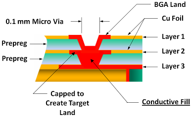  What labcoin would need to do at this point is give out the gerber files for the PCB. Amazingly they've just decided not to show any more pictures at all, which is complete B.S. I completely agree they are destroying their share price long term with this "communications strategy" - no one is going to trust their future statements going forward when good news comes out. |
|
|
|
|
gimme_bottles
|
|
September 14, 2013, 11:59:34 PM |
|
yes, of course you can, but their board is like the open desert. you can place the vias everywhere, so why use costly micro-vias when you could just place the vias beneath the pads. only thing i could think about are thermal optimations, but then thats the wrong package.
|
|
|
|
|
|
Ytterbium
|
|
September 15, 2013, 12:03:37 AM |
|
yes, of course you can, but their board is like the open desert. you can place the vias everywhere, so why use costly micro-vias when you could just place the vias beneath the pads. only thing i could think about are thermal optimations, but then thats the wrong package.
Beats me dude. If I were them I would definitely share more technical information. I guess they want to avoid giving the FUDsters more fuel to make up b.s. but I think that's the wrong strategy. My recommendation would be to give out the gerber files for these boards so everyone can see how they work. Anyway, I've got stuff to do, so won't be able to post for a while. |
|
|
|
dwdoc
Legendary
Offline
Activity: 966
Merit: 1000
- - -Caveat Aleo- - -
|
|
September 15, 2013, 12:05:41 AM |
|
yes, of course you can, but their board is like the open desert. you can place the vias everywhere, so why use costly micro-vias when you could just place the vias beneath the pads. only thing i could think about are thermal optimations, but then thats the wrong package.
Beats me dude. If I were them I would definitely share more technical information. I guess they want to avoid giving the FUDsters more fuel to make up b.s. but I think that's the wrong strategy. My recommendation would be to give out the gerber files for these boards so everyone can see how they work. Anyway, I've got stuff to do, so won't be able to post for a while. Labcoin gerber file image:  |
|
|
|
|
|
Bitcycle
|
|
September 15, 2013, 12:08:35 AM |
|
All this speculation about the PCBs, which is hurting the share price, could be ended with a photo of an assembled and working board.
Why they won't show such a thing is a complete mystery.
|
|
|
|
|
|
CMMPro
|
|
September 15, 2013, 12:21:33 AM |
|
There are no vias on the picture they sent. Check out a photo of Terrahash Avalon clone boards....they look similar but have a few more components. http://www.btcpedia.com/terrahash-avalon-asic-bitcoin-miner/These are very basic "boards" shown, I'm guessing FR4 0.062" standard 2-4 layer boards. Based on the reference designs I've seen so far I'm thinking they are just 2 layer, this isn't rocket science. There is no pcb designer in the world that would decide to route every single one of his traces inside the board through the ground plane shown on the top surface using vias. That would mean that all smd components would have to be mounted on the backside of the board. The only reason we route certain signals to different internal layers is to surround the signal trace with a ground plane to reduce noise, or if the physical real estate is just too tight to get a signal where it needs to go. Someone else mentioned....as a minimum you need decoupling caps close to the power/ground inputs on any chips...as close as possible. Usually I would put them tight to the chip, within 10mm is a general rule. So they decided to put those caps on the backside? Strangest design ever. Anyone who has worked with pcb design knows this is garbage. This looks like what happens the first time you send off a design to a pcb house and get back a pile of unusable laughable crap. That's what I'm guessing happened here...one of their so called engineers learning to use Eagle for the first time and made a big mistake. |
|
|
|
|
mobile
Sr. Member
 Offline
Activity: 400
Merit: 250
the sun is shining, but the ice is still slippery
|
|
September 15, 2013, 12:25:09 AM |
|
Cheap shares yum!  |
1 MoBi1eNbqh8QMuvtZjYzQGV8NEckJJYcT rep| GnuPG <3 CLAM <3 |
|
|
Mabsark
Legendary
Offline
Activity: 826
Merit: 1004
|
|
September 15, 2013, 12:37:08 AM |
|
PEOPLE - please realise that this guy Mabsark will say ANYTHING to get you to keep your money in this stock because he has his btc in it - and almost everything he says about LC he doesn't actually believe himself. He's a liar and has been found out. What a joker huh.
Duh. No surprise he went silent when I started talking about betting on Labcoin actually hashing. If Labcoin aren't hashing, then why are some chips missing from the tray? The obvious reason for those chips being missing is because they are being mined with. It's funny the way none of you FUDsters can come up with a logical argument against this. |
|
|
|
|
|
VolanicEruptor
|
|
September 15, 2013, 12:41:02 AM |
|
I think it's just as likely that the missing chips are being used for mining as they are not.
There is no valid argument either way. They are just missing chips.
|
|
|
|
|
VolanicEruptor
|
|
September 15, 2013, 12:42:28 AM |
|
I should add that the tray looks oddly 1 dimensional. Does anyone else notice this? It looks like it was painted onto the white table (or poorly photoshopped on)
|
|
|
|
dexX7
Legendary
Offline
Activity: 1106
Merit: 1024
|
|
September 15, 2013, 12:43:09 AM |
|
The obvious reason for those chips being missing is because they are being mined with. It's funny the way none of you FUDsters can come up with a logical argument against this.
It might be good to stop this "black and white" thinking. There are several nuances between "Labcoin is not hashing at all" and "Labcoin mines on a large scale". They say they are at an experimental stage, they say they are hashing and optimizing and we also know they are not yet on a productional scale. Edit: I should add that the tray looks oddly 1 dimensional. Does anyone else notice this? It looks like it was painted onto the white table (or poorly photoshopped on)
There is acutally another picture: https://bitcointalk.org/index.php?topic=263445.msg3148724#msg3148724 https://bitcointalk.org/index.php?topic=263445.msg3148974#msg3148974 https://bitcointalk.org/index.php?topic=263445.msg3148974#msg3148974 |
|
|
|
|


